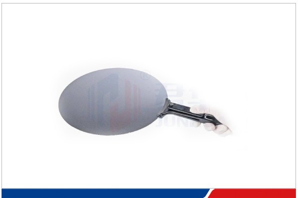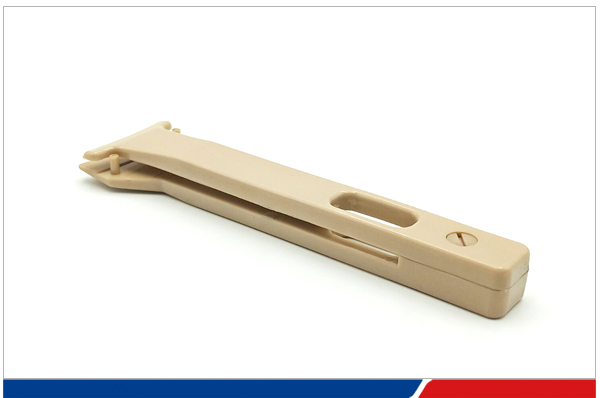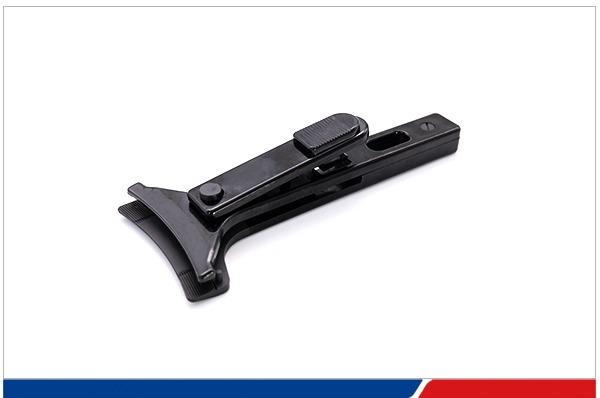
Anti-static PEEK wafer clamp
Wafer holding tool PEEK wafer clamp, a tool for handheld inspection of wafers. PEEK does not contain halogen elements and does not contaminate semiconductor wafers.
In the field of global integrated circuit manufacturing, tight production capacity has become the norm, which has prompted my country’s investment in integrated circuit-related fields to grow significantly in the past two years. This investment boom has not only promoted the vigorous development of semiconductor device equipment, electronic components and electronic special materials manufacturing industries, but also led to a surge in demand for high-performance materials such as PEEK.
PEEK material, with its excellent high temperature resistance, wear resistance, dimensional stability, chemical corrosion resistance and easy processing, has shown unparalleled advantages in the semiconductor manufacturing process. Especially in the field of wafer clamping, PEEK wafer clamps have become an indispensable ideal tool in semiconductor manufacturing with their unique properties. It can not only effectively ensure the integrity of the wafer, but also significantly improve production efficiency and yield. Therefore, in the semiconductor industry, PEEK wafer clamps are receiving more and more attention and are widely used.
The core advantages of PEEK wafer clamps are as follows:
Pollution-free clamping
PEEK wafer clamps are made of modified PEEK granules, which are extremely pure and contain almost no trace elements that may contaminate silicon wafers, ensuring absolute safety during the clamping process.
The anti-static protection
PEEK wafer clamp has excellent anti-static properties. Its surface resistivity can reach 10^5-10^10Ω, and the clamping part is as high as 10^7-10^8Ω, which effectively prevents the damage to the silicon wafer caused by instantaneous electrostatic discharge and provides all-round protection for the wafer.
High temperature stability
PEEK wafer clamps can be used for a long time in a high temperature environment of 260°C, and maintain high strength, dimensional stability and a small linear expansion coefficient. It has excellent resistance to sliding wear and fretting wear, and will not produce scratches or residues on the surface when clamping wafers and silicon wafers, thus ensuring the surface cleanliness of wafers and silicon wafers.
It is worth mentioning that the PEEK5600ESDZ01 granules we developed, as an antistatic material designed specifically to solve the problem of static electricity, have a stable and controllable surface resistivity that can meet the requirements of 10^5-10^9Ω. This material has excellent performance in antistatic properties, easy processing and appearance, and is widely used in the electronics industry, semiconductors, petroleum industry and other fields, effectively reducing the losses caused by static electricity. In addition, the antistatic granules are also used in the shells and structural parts of explosion-proof products, such as the shells and structural parts of electrical products in coal mines, oil tankers, oil fields and other occasions, showing a wide range of application prospects and huge market potential.
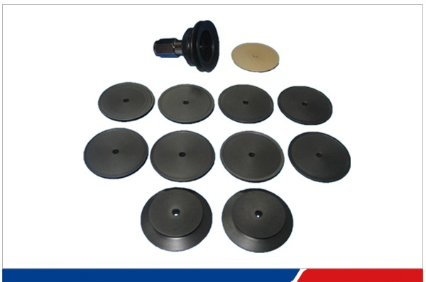
Commonly used PEEK wafer clamps are injection molded from PEEK5600G pure resin and are available in sizes of 4 inches, 5 inches, 6 inches, 8 inches, and 12 inches.

PEEK wafer clamps and silicon wafer tweezers can be used for a long time at a temperature of 260°C. They can maintain high strength at high temperatures, have good dimensional stability, and a small linear expansion coefficient. At the same time, they have excellent properties such as resistance to sliding wear and fretting wear, and a low friction coefficient. When using PEEK wafer clamps to clamp wafers and silicon wafers, no scratches will be caused on the surface of the wafers and silicon wafers, and no residue will be produced on the wafers and silicon wafers due to friction, thereby improving the surface cleanliness of the wafers and silicon wafers.
PEEK polymer is a high-performance thermoplastic whose excellent comprehensive properties are specially designed to meet the increasing requirements of the electronics industry.
1. High temperature resistance : With heat resistance up to 320°C, it can maintain its strength and dimensional stability at high temperatures of lead-free soldering processes. At temperatures of 250-280°C, there will be no deformation accompanied by reflow within 5-10 seconds;
2. Wear resistance : High mechanical strength and wear resistance;
3. Dimensional stability : Filler-grade materials reduce the coefficient of thermal expansion and increase the heat deformation temperature, which can ensure strict dimensional control;
4. Low outgassing : Reduces contamination and improves the reliability of accessories in applications where purity is required (such as hard drives, wafer boxes);
5. Low hygroscopicity : Very important for maintaining dimensional stability and insulation properties.
Contact Us Now and Enjoy a One-Stop Solution!
Fill the Form to Get a Quote, Product Manual, Performance Parameters, Custom Solutions, Technical Consultation, and Samples