作者: junhua
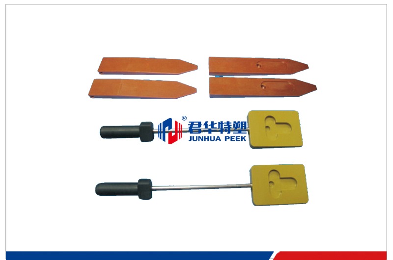
PEEK vacuum suction pen rod and head
PEEK vacuum pen holder and head
2025-02-26 | PEEK wafer clip, suction pen, suction cup |
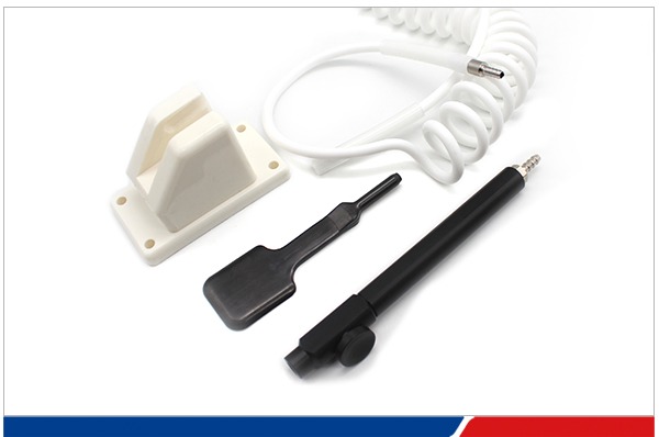
PEEK vacuum suction pen head and suction pen rod
PEEK vacuum pen tip and pen holder Application: For 2-8 inch semiconductor wafers or LED epitaxial wafers. Component form: Direct plug-in/threaded Features and advantages: Instantaneous temperature resistance 320℃, continuous temperature resistance 250℃ Vacuum seamless adsorption High purity, no halogen elements, no pollution to semiconductor materials Chemical resistance High strength, wear resistance Can be upgraded to anti-static PEEK With the increase of wafer size and integrated circuit density, as well as the improvement of manufacturing environment requirements and pollution source sensitivity in the electronic semiconductor industry, the use of PEEK high-performance polymer materials has become a very necessary and effective measure.
2025-02-26 | PEEK wafer clip, suction pen, suction cup |
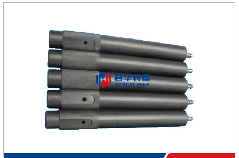
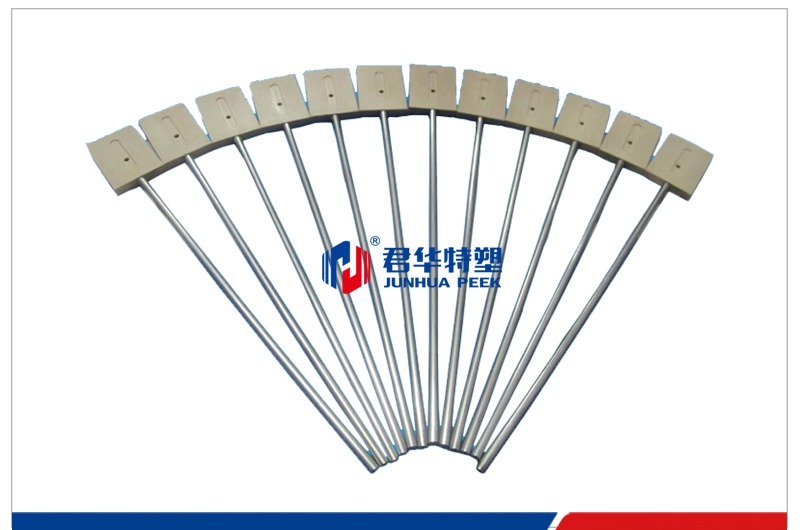
PEEK vacuum suction pen rod
PEEK vacuum suction pen rod
2025-02-26 | PEEK wafer clip, suction pen, suction cup |
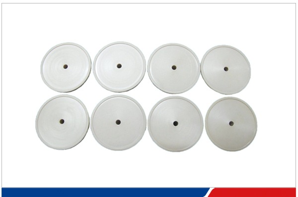
PEEK vacuum traceless suction cup
PEEK vacuum traceless suction cup
2025-02-26 | PEEK wafer clip, suction pen, suction cup |
Thermosetting PI, PEEK, PAI, POM vacuum suction pen
Thermosetting PI, PEEK, PAI, POM and other suction pen tips (if anti-static is required, it can also be processed by mixing ingredients), in addition to high temperature resistance, low friction, and excellent electrical performance, its convenient structural design makes it particularly convenient and simple to pick up electronic parts and small products through a manual vacuum suction pen. It is small in size, but has strong suction, moves quickly and lightly, and will not contaminate the surface of the product. Vacuum suction tips are available in a variety of sizes to accommodate chips of different sizes.
2025-02-26 | PEEK wafer clip, suction pen, suction cup |
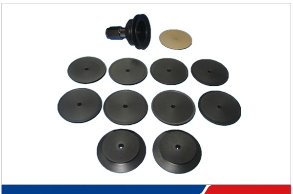
PEEK vacuum suction cup
Previously, the most commonly used suction cups in LCD glass substrate production lines were nitrile rubber suction cups. Although they can generate sufficient suction force after a limited number of uses, the heat aging resistance and corrosion resistance of nitrile rubber are relatively poor. Long-term use will cause the nitrile rubber to soften, leaving traces on the surface of the substrate, or even fail. Such traces often require chemical reagents to be completely removed, which will cause long downtime and high scrap rate of substrates. The new PEEK seamless vacuum suction cup can solve the above problems well and has greater advantages: 1. High temperature resistance, long-term use at 260°C, can fully meet the high temperature requirements of the production…
2025-02-26 | PEEK wafer clip, suction pen, suction cup |
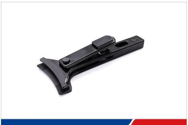
Anti-static PEEK wafer clamp
Wafer holding tool PEEK wafer clamp, a tool for handheld inspection of wafers. PEEK does not contain halogen elements and does not contaminate semiconductor wafers. In the field of global integrated circuit manufacturing, tight production capacity has become the norm, which has prompted my country’s investment in integrated circuit-related fields to grow significantly in the past two years. This investment boom has not only promoted the vigorous development of semiconductor device equipment, electronic components and electronic special materials manufacturing industries, but also led to a surge in demand for high-performance materials such as PEEK. PEEK material, with its excellent high temperature resistance, wear resistance, dimensional stability, chemical corrosion resistance and easy processing, has shown unparalleled advantages in the semiconductor manufacturing…
2025-02-26 | PEEK wafer clip, suction pen, suction cup | Tags: Wafer clamp
PEEK bus bar
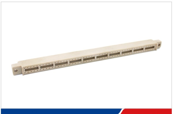
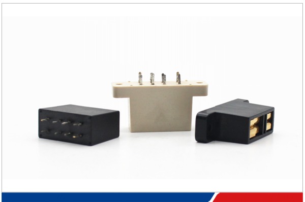
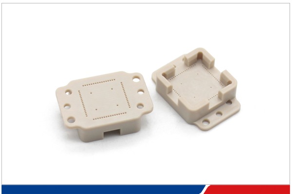
PEEK test socket IC test sockets (test sockets, test sockets) are important fixtures in semiconductor testing. They provide a reliable, mechanically stable connection point, allowing testers to test chips and check for manufacturing defects and component failures without the need for permanent soldering or mounting on circuit boards. When IC chips are tested in single chip, a test socket with stable dimensions at high temperature and capable of withstanding thousands of contact frictions is required. IC test sockets made of PEEK have the following advantages: 1. PEEK can withstand high static loads at high temperatures and has stable high bandwidth, low resistance and low inductance. 2. PEEK can maintain good dimensional stability in a wide temperature range, can work at…
2025-02-26 | PEEK IC Test Socket |
PPS Test Socket
PPS Test Socket IC test sockets (test sockets, test sockets) are important fixtures in semiconductor testing. They provide a reliable, mechanically stable connection point, allowing testers to test chips and check for manufacturing defects and component failures without the need for permanent soldering or mounting on circuit boards. When IC chips are tested in single chip, a test socket with stable dimensions at high temperature and capable of withstanding thousands of contact frictions is required. IC test sockets made of PEEK/PPS material have the following advantages: 1. PEEK/PPS can withstand high static loads at high temperatures and has stable high bandwidth, low resistance and low inductance. 2. PEEK/PPS can maintain good dimensional stability in a wide temperature range, adapt to…
2025-02-26 | Products |
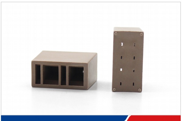
PEEK CPU hot and cold test parts
PEEK test socket IC test sockets (test sockets, test sockets) are important fixtures in semiconductor testing. They provide a reliable, mechanically stable connection point, allowing testers to test chips and check for manufacturing defects and component failures without the need for permanent soldering or mounting on circuit boards. When IC chips are tested in single chip, a test socket with stable dimensions at high temperature and capable of withstanding thousands of contact frictions is required. IC test sockets made of PEEK have the following advantages: 1. PEEK can withstand high static loads at high temperatures and has stable high bandwidth, low resistance and low inductance. 2. PEEK can maintain good dimensional stability in a wide temperature range, can work at…
2025-02-26 | PEEK IC Test Socket |
PEEK IC Test Socket
PEEK test socket IC test sockets (test sockets, test sockets) are important fixtures in semiconductor testing. They provide a reliable, mechanically stable connection point, allowing testers to test chips and check for manufacturing defects and component failures without the need for permanent soldering or mounting on circuit boards. When IC chips are tested in single chip, a test socket with stable dimensions at high temperature and capable of withstanding thousands of contact frictions is required. IC test sockets made of PEEK have the following advantages: 1. PEEK can withstand high static loads at high temperatures and has stable high bandwidth, low resistance and low inductance. 2. PEEK can maintain good dimensional stability in a wide temperature range, can work at…
2025-02-26 | PEEK IC Test Socket |
PEEK IC SOCKET
PEEK test socket IC test sockets (test sockets, test sockets) are important fixtures in semiconductor testing. They provide a reliable, mechanically stable connection point, allowing testers to test chips and check for manufacturing defects and component failures without the need for permanent soldering or mounting on circuit boards. When IC chips are tested in single chip, a test socket with stable dimensions at high temperature and capable of withstanding thousands of contact frictions is required. IC test sockets made of PEEK have the following advantages: 1. PEEK can withstand high static loads at high temperatures and has stable high bandwidth, low resistance and low inductance. 2. PEEK can maintain good dimensional stability in a wide temperature range, can work at…
2025-02-26 | PEEK IC Test Socket |