PEEK Solutions across Electronic Industry
PEEK Solutions across Electronic Industry
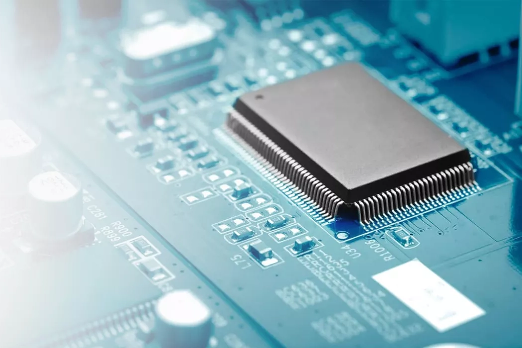
PEEK is widely used on consumer electronics, home appliances and semiconductor products for
electronic industry. PEEK polymers can withstand continuous use high temperatures and harsh
chemicals, modified peek provide a range of electrically conductive, anti-static or static
dissipative properties, these characteristics are important for semi-conductor applications
such as vacuum traceless sucker.
JUNHUA® PEEK solution to suit every environment and meets the strictest requirements, based
components have a proven cost less than traditional materials, such as replacing metal with
integrated PEEK components can improve energy efficiency in appliances up to 2% by weight
reduction, help increase fab productivity up to 3% with longer lifetime than PPS.
Team up with JUNHUA® PEEK to address your challenges in the ever-changing electronics
industry.
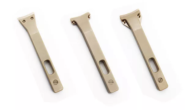
PEEK Parts
Explore JUNHUA® PEEK Parts Benefits
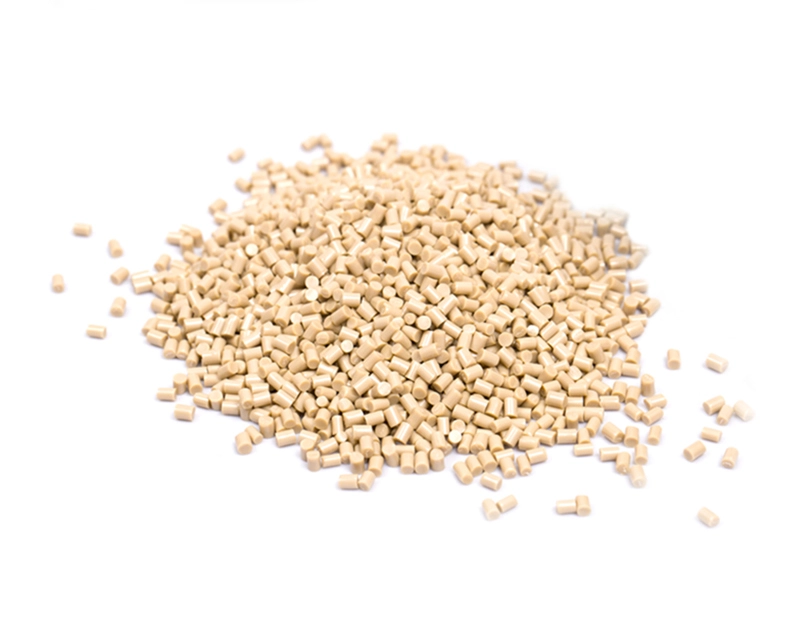
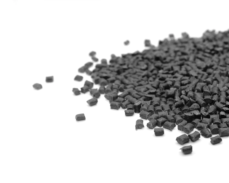
PEEK5600G
Excellent processability and toughness, suitable for thin-walled products.
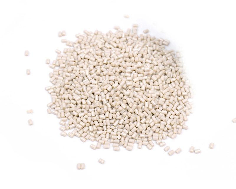
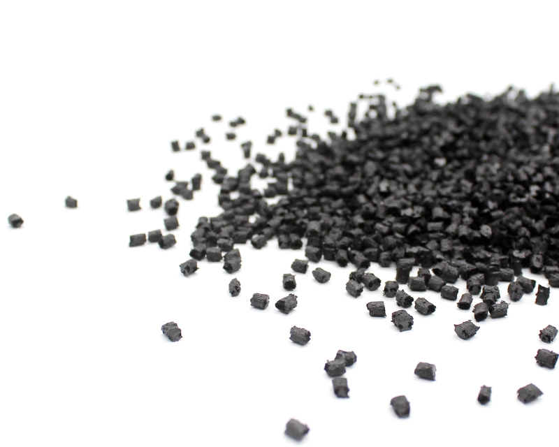
PEEK5600GF30
High strength and high modulus, suitable for pressure vessels or occasions with high-pressure requirements.
PEEK5600CF30
Carbon fiber reinforced PEEK with excellent mechanical properties.
PEEK5600LF30
With excellent wear resistance, it is suitable for high-speed, high-load applications.
Explore our PEEK-type Solutions
Explore our PEEK-type Solutions
PEEK has many advantages in the field of electrical semiconductors:
- Very high temperature resistance (up to 260°C continuous operating temperature)
- Excellent chemical resistance
- Good dimensional resistance (low thermal expansion)
- Optimal ratio of stiffness, solidity, toughness and minimal tendency to creep
- Very good tribological properties
- Good radiation resistance
- Excellent resistance to hydrolysis
- Fire performance: flame-retardant, Low smoke density, No toxic gases
- Good machinability
- Good bondability and weldability
Contact us for more information and services.
Contact us Now, Get a Quote, Product Manual, Performance Parameters, Custom Solutions, Technical Consultation, and Samples for PEEK Materials!
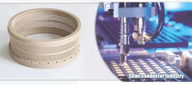
CASE STUDY - CMP Ring
CASE STUDY - CMP Ring
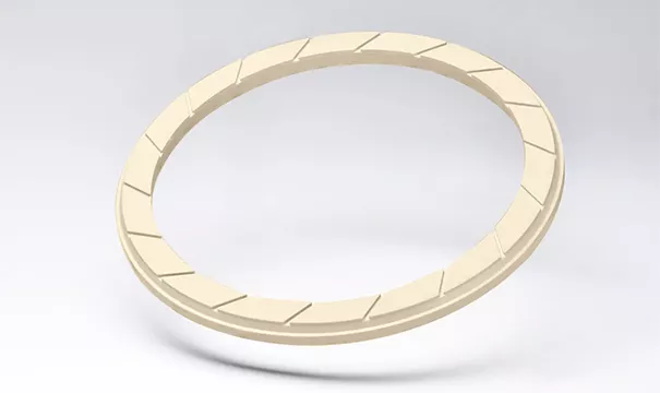
CASE STUDY - CMP Ring
A very important step in silicon wafer production is the Chemical Mechanical Planarization (CMP) process. The trend is towards larger wafer sizes, smaller chips with narrower line widths and feature sizes. The challenge is to find a material with the desired characteristics, as the CMP process requires components made of highly qualified materials. In close cooperation with customers, we have specialised in developing materials that meet these requirements.
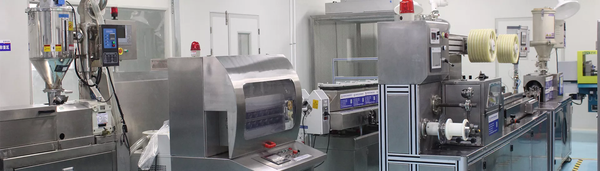
Product Processing and Quality Control Capability
Product Processing and Quality Control Capability
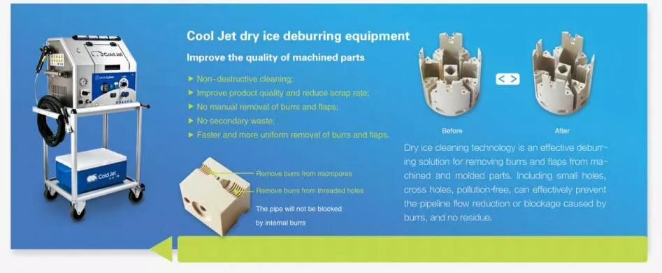
Cool Jet dry ice deburring equipment lmprove the quality of machined parts
- Non-dastuntive cleanina;
- Improve product quality and reduce-scrap rate;
- No manual removal of burrs and Haps;
- No secondary waste;
- Faster and more uniform removal of bums and flaps.
100,000-level cleaning workshop
Our company has established a 280-square-meter, 100,000-level cleaning workshop and equipped with 100-level cleaning area accordance with GMP requirements.
Our Clients
Explore Our Partner


Certificate
Certificate & Compliance


Contact
Contact Us
Fill the Form to Get a Quote, Product Manual, Performance Parameters, Custom Solutions, Technical Consultation, and Samples for PEEK Materials!